



Semanta
An intelligent R&D platform for semiconductors
Integrated support from data accumulation and knowledge organisation to computational analysis
Semanta integrates literature parsing, knowledge graphs, database search, device scheme design, multiscale simulation, active learning, characterisation analysis and report generation, and can query MatToken's dual-track materials-and-device database. It carries the full chain — data accumulation, knowledge discovery, scheme generation, computational validation and R&D decisions — for semiconductor and advanced polymer development.


MatToken
A multimodal reasoning database for semiconductors
Over 100,000 domain papers, structured into more than a million materials R&D and device fabrication schemes.
MatToken is a reasoning-driven multimodal database for semiconductor R&D. Centred on the PSPP link — process, structure, property, performance — it connects composition, crystal structure, defects, physical properties, device structure, fabrication, test conditions and device performance.

Gnosys
The agent foundation platform
Enterprise agent delivery for materials R&D
Gnosys is an agent foundation platform for enterprises: knowledge and database building, on-premise deployment, high-throughput compute scheduling, data security and lab equipment integration, turning years of R&D assets into callable AI capability, with literature extraction accuracy up to 95%. It already works with key semiconductor R&D laboratories on a billion-document data foundation.

Poly-Studio
Polymer AI computing platform
Structure, formulation and process optimised together.
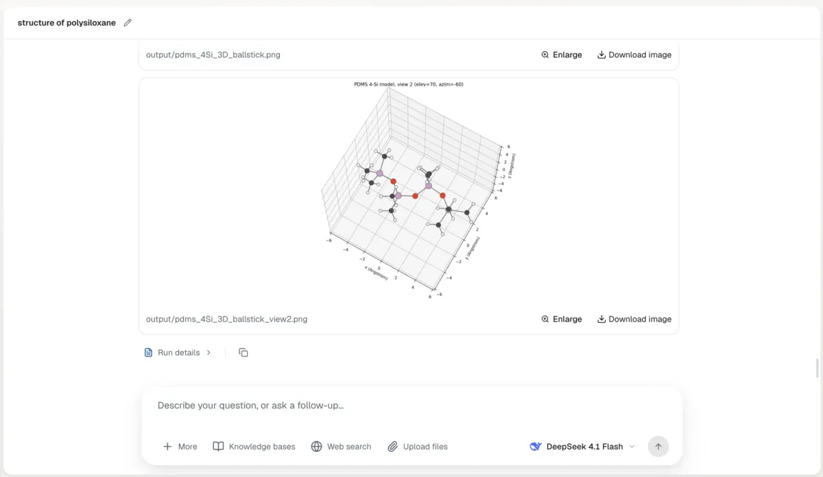
Poly-Studio relates polymer molecular structure, formulation, processing and performance, integrating molecular modelling, cross-linked networks, all-atom and coarse-grained molecular dynamics, machine-learned potentials, property prediction, active learning and formulation optimisation across scales from monomers to cross-linked materials. It predicts glass transition, thermal conductivity and expansion, dielectric and mechanical properties, interfacial adhesion, diffusion, rheology and curing, and supports raw-material screening, process-window optimisation and R&D reporting for advanced packaging adhesives, thermal and insulating materials and low-dielectric composites.


ZetaLab
Self-driving smart laboratory
An AI-driven pilot line for enterprise R&D
ZetaLab is an AI-driven, self-driving pilot line for enterprise R&D, closing the loop over formulation, process parameters and performance through high-throughput synthesis, automated characterisation and machine-learning optimisation. We run our own semiconductor thin-film smart lab, and have built an advanced packaging adhesive lab with a leading packaging company, a high-throughput synthesis lab with a CAS institute, and a joint tape-out process application with a microelectronics institute.


Process packages & new material delivery
Materials development and validation, aimed at application
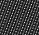
Across functional ferroelectric thin films, advanced packaging adhesives, and optoelectronic and quantum-dot semiconductors, we deliver candidate materials, process advice, validation plans, samples or IP collaboration. Knowledge hypergraphs and generative inverse design produce candidate materials, process routes and validation plans for a given performance target, reasoning over composition, structure, fabrication conditions and application scenarios with materials and process databases, knowledge graphs and our own models.
Advancing materials R&D with industry and academic partners.
Project collaboration & research
 CIOMP
CIOMP Suzhou Institute of Future Industry
 JLU
JLU SJTU
SJTU XJTLU
XJTLU NJUST
NJUST
Academic advisory network
 TU Darmstadt
 Imperial College London
 THU
THU PolyU
PolyU
Milestones
From a set of tools to materials intelligence infrastructure.
We have an exceptional science and engineering team.Chief Scientists & Core Team
We work with Software Experts
Chief Scientists
Zhang Lijun
Jilin University, MSEDean and Professor
Zhang Hongbin
TU Darmstadt, M&EProfessor
Leadership Team
Shen Chen
Chairman & Founder
Gao Feng
CEO
Wang Xiang
General Manager
Wu Zhenghao
CTO
Zhou Chang
CSO
Research Team
Sun Yuanhui
Materials Design Sci.
Fan Zipei
AI Research Sci.
Wang Xinjiang
Materials Sci.
Wang Xiaoyu
Materials Alg. Sci.
Zhou Kun
Materials Alg. Sci.
Li Tianshu
Materials AI Sci.
Engineering Team
Hu Lei
Platform Architect
Gao Quanyan
AI Research Eng.
Contact ZetaMat
Let’s advance materials R&D together.
We welcome conversations with R&D teams, university laboratories, and industry partners.
- semanta@126.com
- Phone
- +86 188 9671 9938